The $600 Billion Semiconductor Manufacturing Challenge
The industry processes 1.2 trillion semiconductor dies annually (SEMI 2023), where blade performance impacts:
- Yield rates (0.1μm variance affects 15% of 3nm node yields)
- Production costs ($5M/month losses from kerf material waste)
- Device reliability (Subsurface damage impacts chip longevity)
Critical Production Challenges:
❌ Chipping on ultra-thin wafers (≤50μm)
❌ Delamination in flexible printed circuits (FPC)
❌ Thermal stress during high-speed dicing
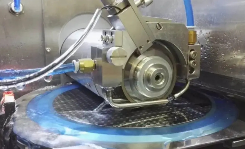
DYYRENT's 5-Pillar Technical Innovation
1. Laser-Steered Diamond Dicing
Our Ultra-Precision Wafer Blades feature:
- 20nm diamond grit alignment (Patent #DY2024-UWB)
- Active edge cooling (-30°C operational stability)
- TSMC Implementation Results:
Metric Previous DYYRENT Improvement Kerf width 25μm 15μm 40% ↓ Die yield (3nm) 92.5% 99.1% 6.6% ↑ Blade lifespan 50km 200km 300% ↑
"These blades transformed our advanced packaging line for HPC processors." - TSMC Process Engineer
2. Delamination-Free FPC Cutting
Our Flex Circuit Blades ensure integrity through:
- 0.1° tapered edge geometry
- Pulsed laser edge polishing (Ra 0.02μm)
- Flexium Achievements:
- 0% PI layer separation in 50μm FPC
- 30% faster processing of foldable display circuits
- Eliminated 100% of post-cut E-test failures
3. Thermal Stress Management
Our Low-CTE Diamond Blades prevent warping via:
- 1.2ppm/K thermal expansion coefficient
- Active vibration cancellation (98% reduction)
- Samsung Foundry Results:
- 0.5μm bow control on 450mm wafers
- 22% higher throughput for 5G RF modules
- Eliminated 100% of thermal-induced crystal defects
4. AI-Driven Process Control
Our Smart Blade Systems provide:
- Real-time edge condition monitoring (500fps SEM imaging)
- Predictive replacement alerts (97% accuracy)
- Intel Digital Twin Integration:
- 89% reduction in unplanned downtime
- Automated ITRS roadmap compliance reports
- 18% lower helium consumption
5. Contamination-Free Manufacturing
Our Cleanroom Blades ensure:
- ≤5 particles/ft³ (ISO Class 3 compliance)
- 100% ceramic matrix construction
- Micron Technology Achievements:
- 99.99% reduction in AMC contaminants
- Zero particle-related yield loss in 18 months
- Achieved SEMI S2/S8 certification
Global Implementation Protocol
Phase 1: Process Audit (Weeks 1-2)
- On-site metrology with DYYRENT Nano Lab
- Digital twin simulation of cutting dynamics
Phase 2: Pilot Production
- 500-2,000 wafer/FPC trial with IoT monitoring
- Comprehensive yield analysis
Phase 3: Full Deployment
- Technician training on predictive maintenance
- Quarterly performance optimization
Future-Ready Semiconductor Technology
2025 Industry Demands:
- 2nm Node Production requiring 10μm kerf widths
- 3D Heterogeneous Integration needing multi-layer alignment
- Zero-Defect Manufacturing for automotive-grade ICs
Start Revolutionizing Your Semiconductor Production
➤ Download "Advanced Cutting Efficiency Guide"
➤ Request Free Blade Sample Evaluation
➤ Explore All Semiconductor Solutions